A few months back I saw the RoMac and Plaid (resp) keyboards on Reddit.
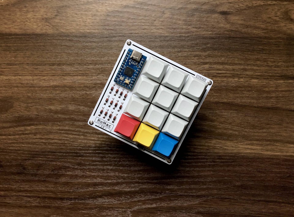
I’m a big fan of the exposed design and have been missing a numberpad on my S65-X. I took that as a sign that a macropad was a need (not a want) and that I would be best off designing my own.
I started with the following requirements for design:
- Perfectly square
- All directly mounted components (no breadboards)
- 12 keys
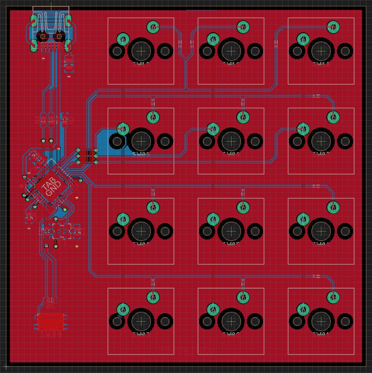
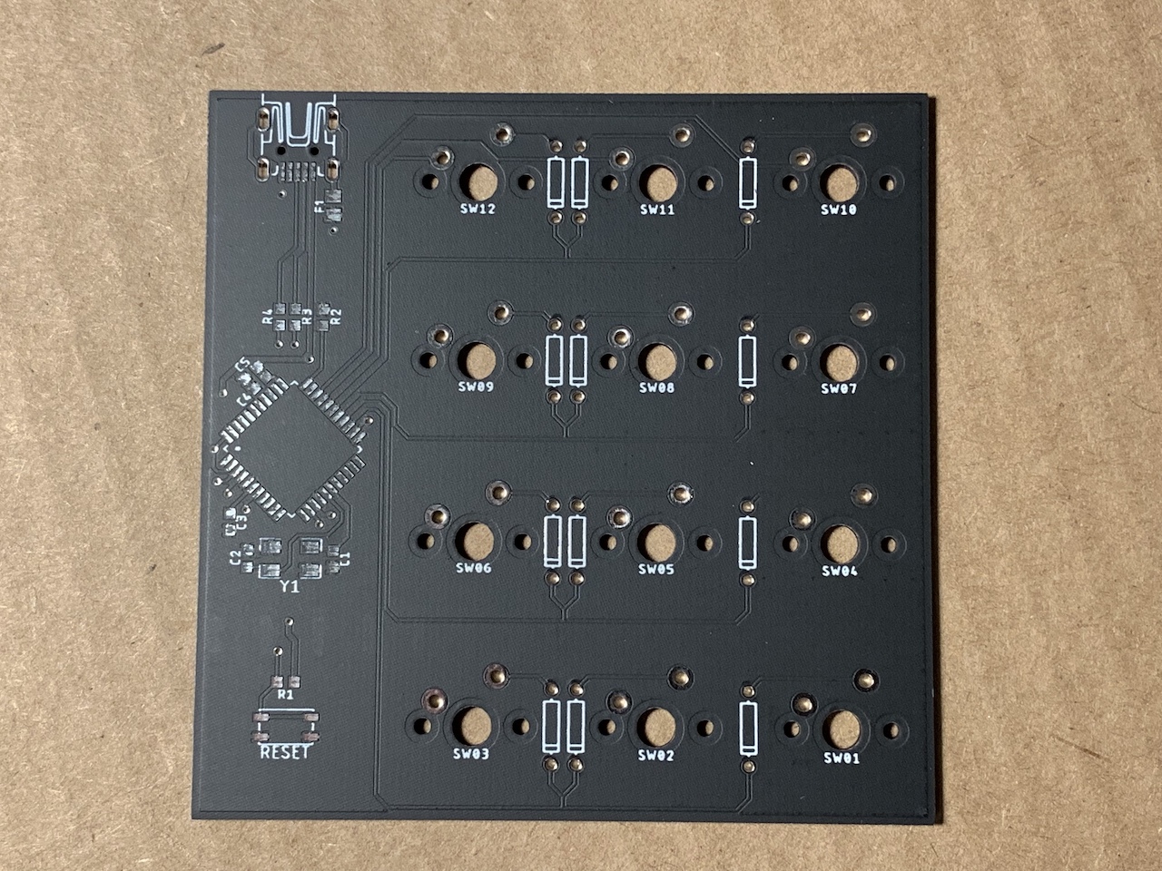
With a 12 key (4x3 layout) I could theoretically have a perfectly square board if the length of one size was equal to the space 4 keys would need. That would leave a 1x4 footprint (in switch units) for the other components.
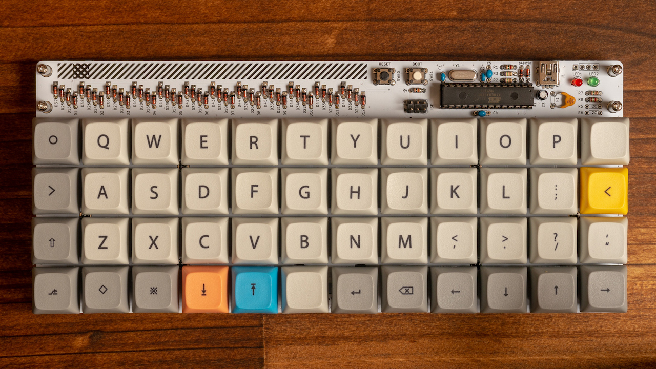
I started playing with component sizes and alignment in Eagle, and it was obvious almost immediately that I’d have to use surface mount components. To keep the board square and avoid padding, it was really the only way to get everything to fit. I did not have nearly the amount of space that the Plaid has along the top of the board.
I selected a QFN ATMEGA32 and designed a circuit around that. The r/PCB community on Reddit was extremely helpful and gave me great advice for tuning and polishing the first version of the board.
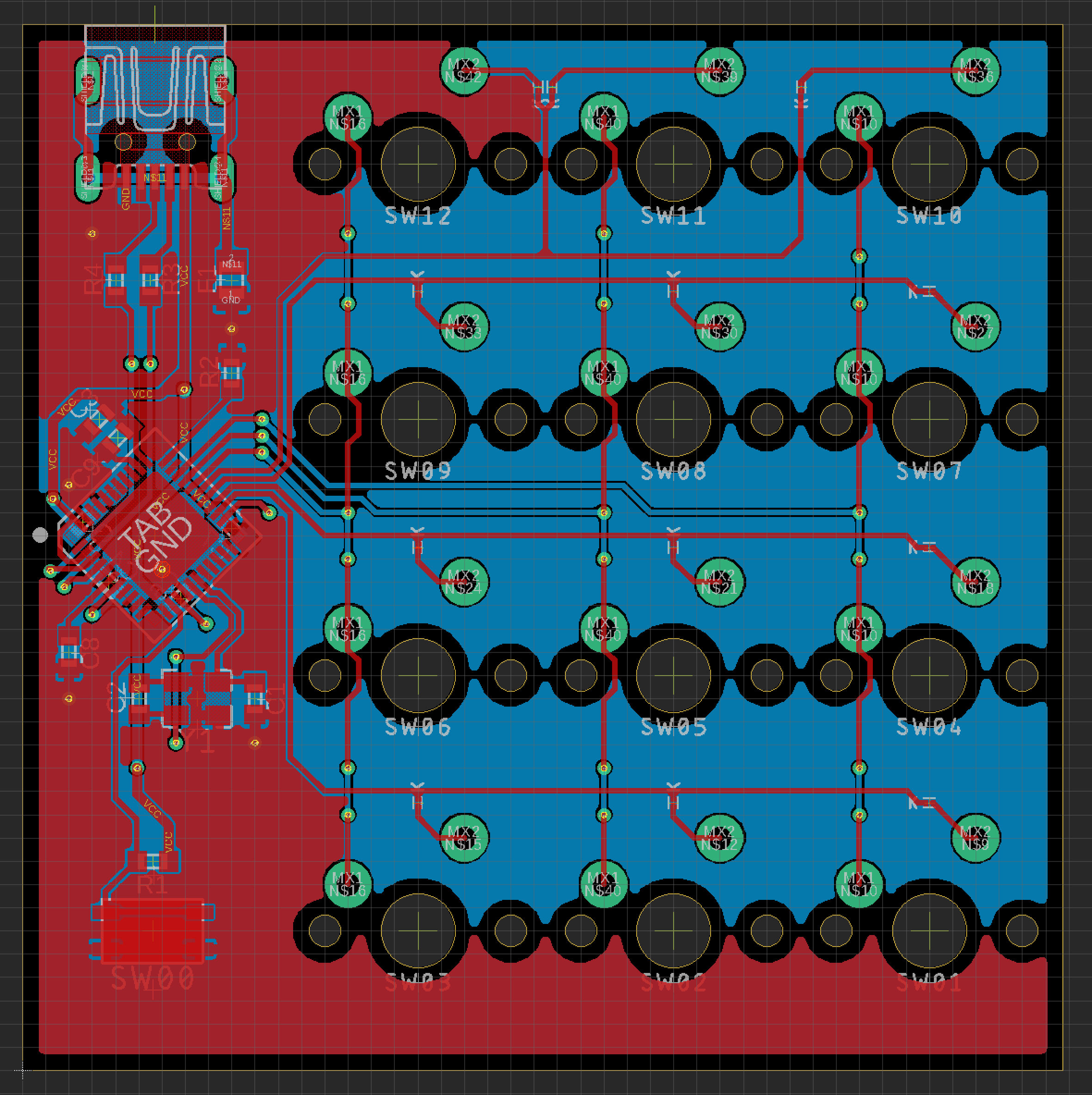
If you know anything about switch footprints, you’ll immediately see something off about those designs. I had a nice looking design, but when I went to upload it to JLCPCB it was listing the physical size as 60x60mm. Measuring against the keyboard at my desk, that was only about 3.15 keys long. Certainly not the 4x(3+1) sizing that I was going for and had expected.
When I had downloaded the component library, I had assumed that the components should sit next to each other. That was a naive assumption, and as I spent more time in the tools it became clear how hard it would be to place components if all the footprints included both the physical size and padding.
Cherry MX switches have a footprint of about 15mm, but need about 19mm for the keycaps and clearance between the switches. After redesigning the boards again in my giant 76mm x 76mm space, I ended up with the following design, which I sent off to be printed.
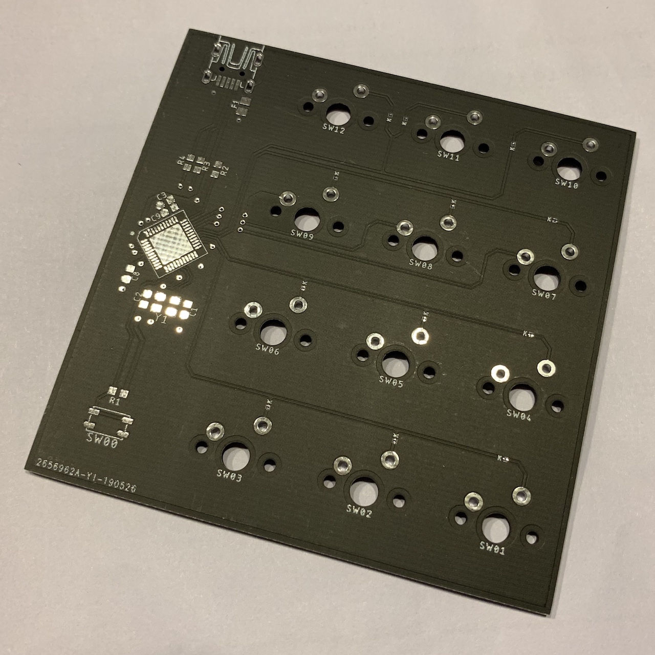
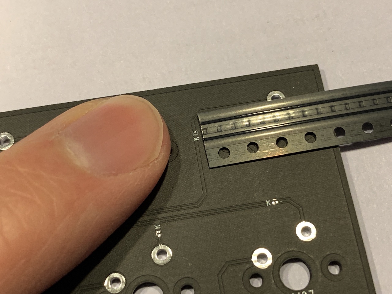
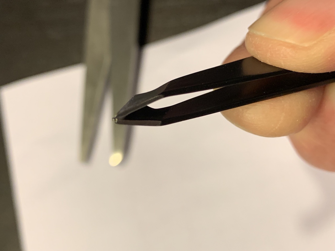
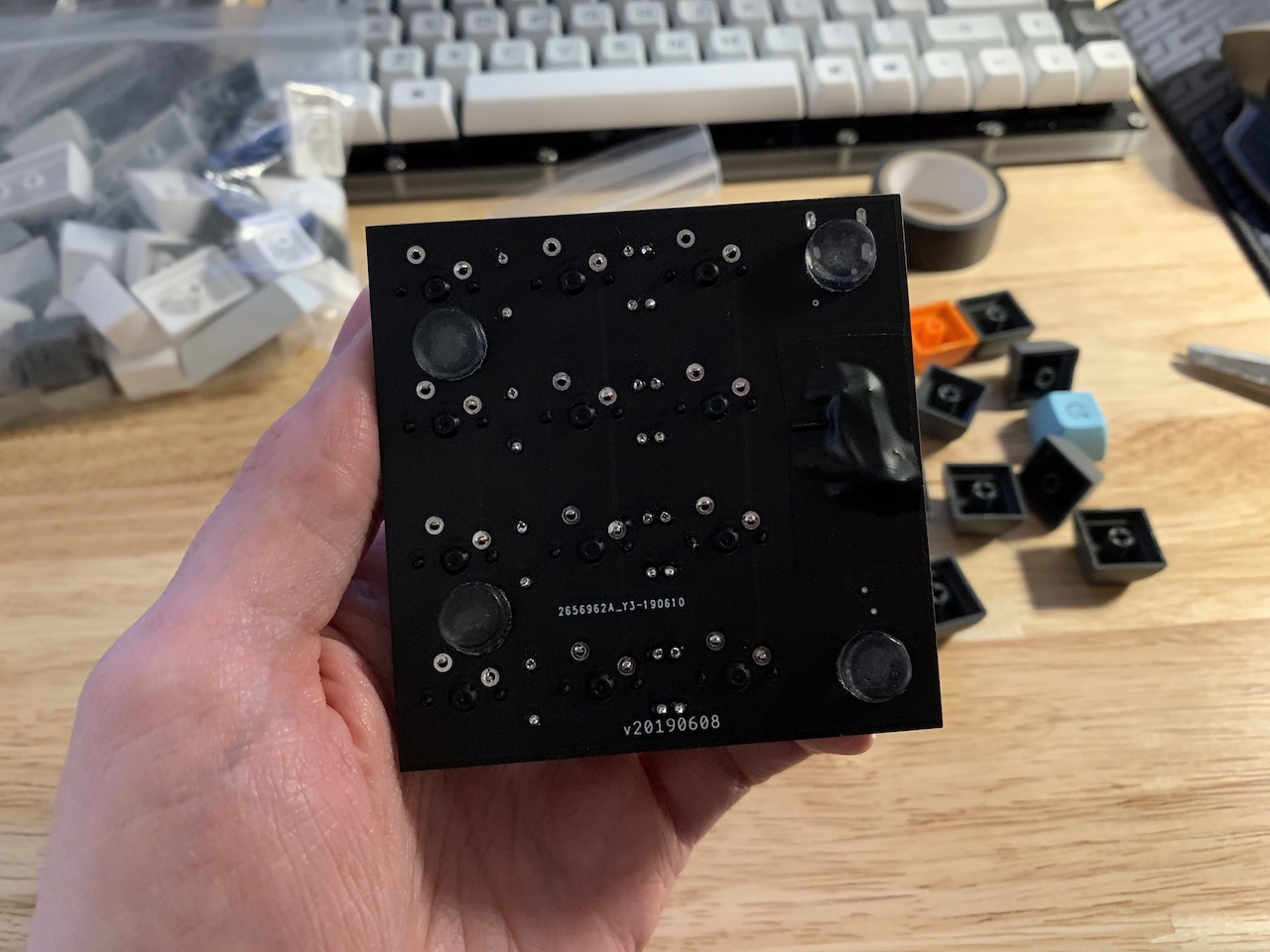
The boards that came back looked great, but were impossible to solder by hand. I had accidentally designed with and ordered 0603 metric diodes.
In the picture below, the small square next to my finger is where the diode is supposed to sit (with orientation). There was no way I could assemble that with a plain magnifying glass and soldering iron.
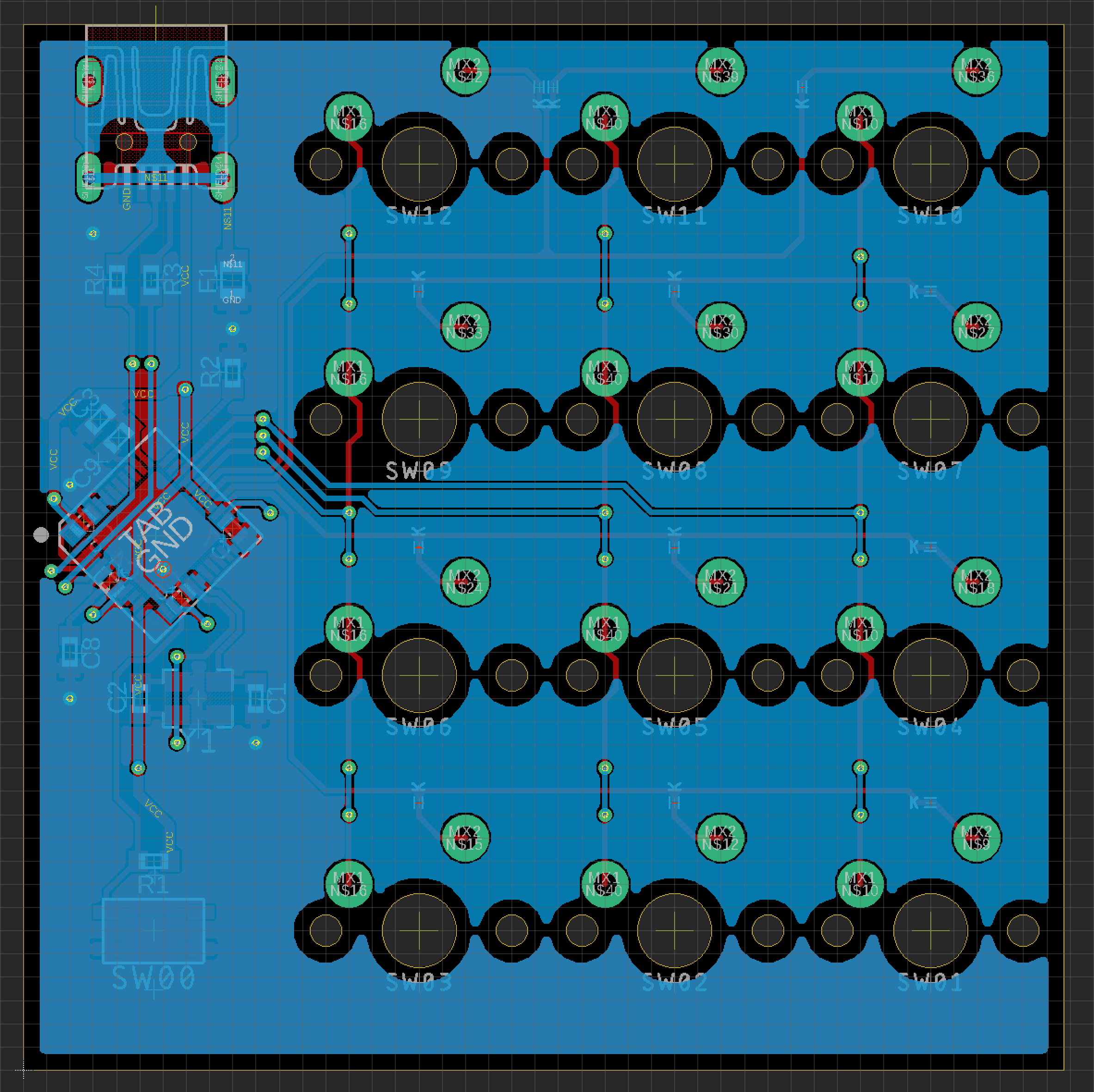
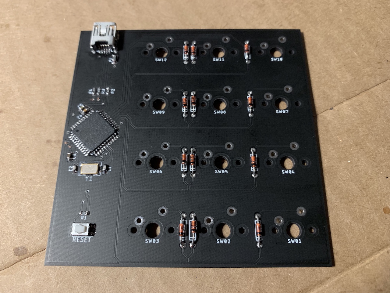
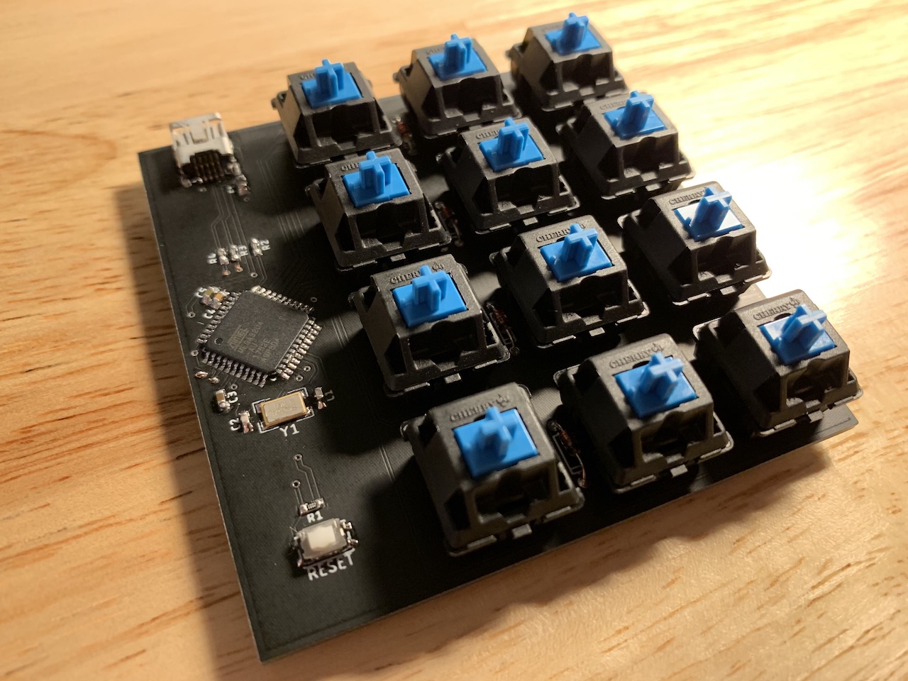
For the second board revision I made the following major changes:
- ATMEGA32 QFN package to ATMEGA32 TQFP
- 0603 metric diodes to through-hole
- mini-a usb master socket to mini-b
- 2.5x3.2 to 3.2x5 crystal package
These changes all circle around larger package sizes and corrections to incorrect component <-> footprint selections.
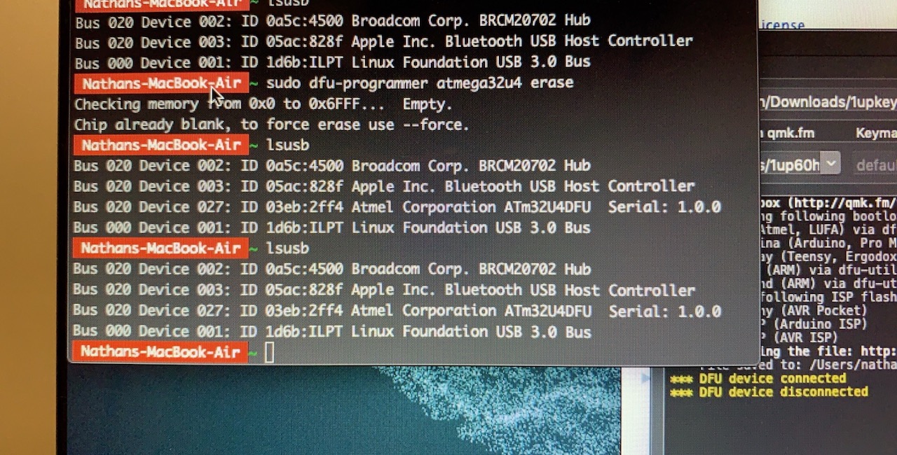
Soldering the second revision of boards was much easier. I put the parts on and connected it to my computer and saw… nothing. These chips are supposed to come with hot usb drivers and are plug and play with pretty much any computer.
To make sure I didn’t have a bad chip, I soldered another complete board and… still nothing.
This was bad. It’s one thing to have component selection issues and have to order new parts, and it’s one thing to have it connect to a computer and have timing issues or issues with some part of the lattice. To just do nothing makes it much harder to make an incremental step forward.
I shared the schematic with friends. I opened up a ticket online. I spent a lot of time verifying every connection on the schematic against the component datasheets. I was very worried that this would just be the end of the project.
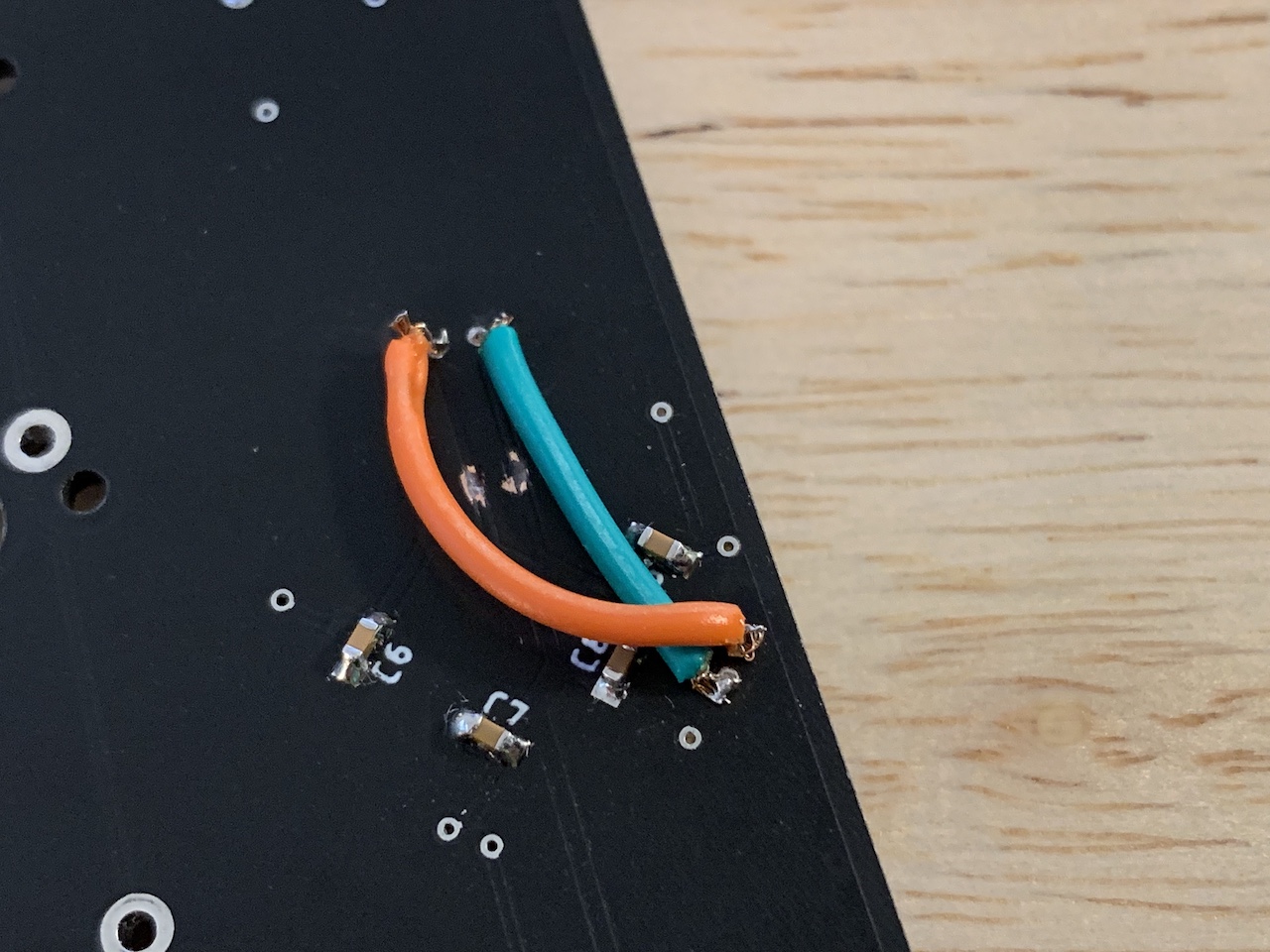
Either during the switch from a QFN to TQFP package, or from the start I had swapped the positive and negative usb data lines. I found this while verifying all of the traces and routing against the chip’s datasheet. I wanted to make sure that the component I was using in Eagle was actually using the right pins. Luckily this didn’t damage the computer or chip, it just kept them from being able to communicate. A few hours later someone responded to the ticket online and had identified the same problem. I’m glad I found the issue myself, but regardless it’s great to know that I would have been able to move forward.
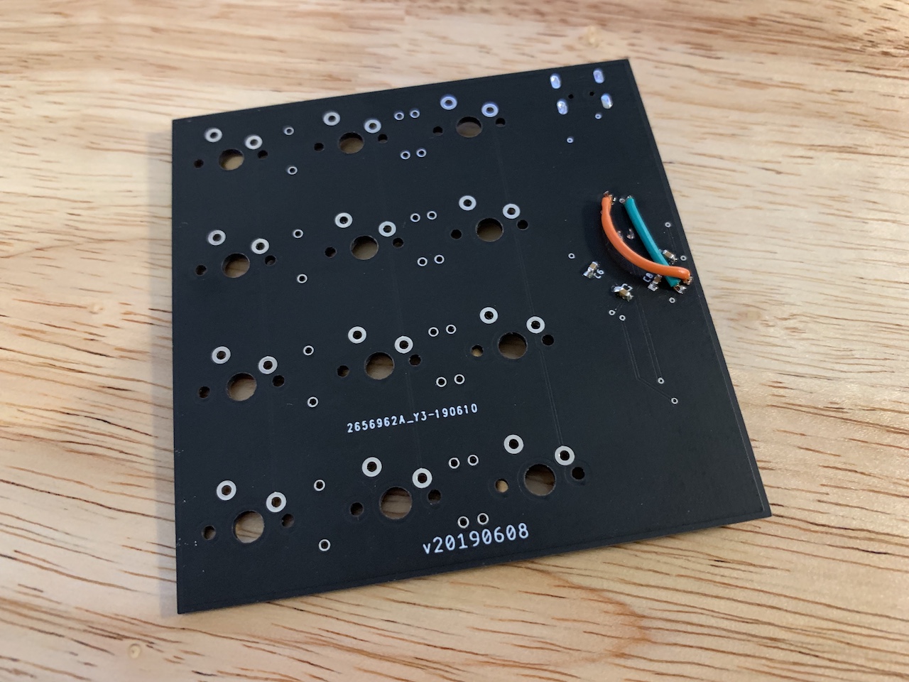
I’m also lucky that those two lines both go across the bottom of the board to get from the USB port to the opposite side of the chip. That meant that I could flywire a fix and keep the aesthetic of the top layer intact.
After doing that the chip connected and was viewable as an active USB device!
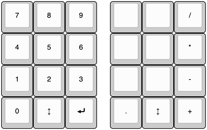
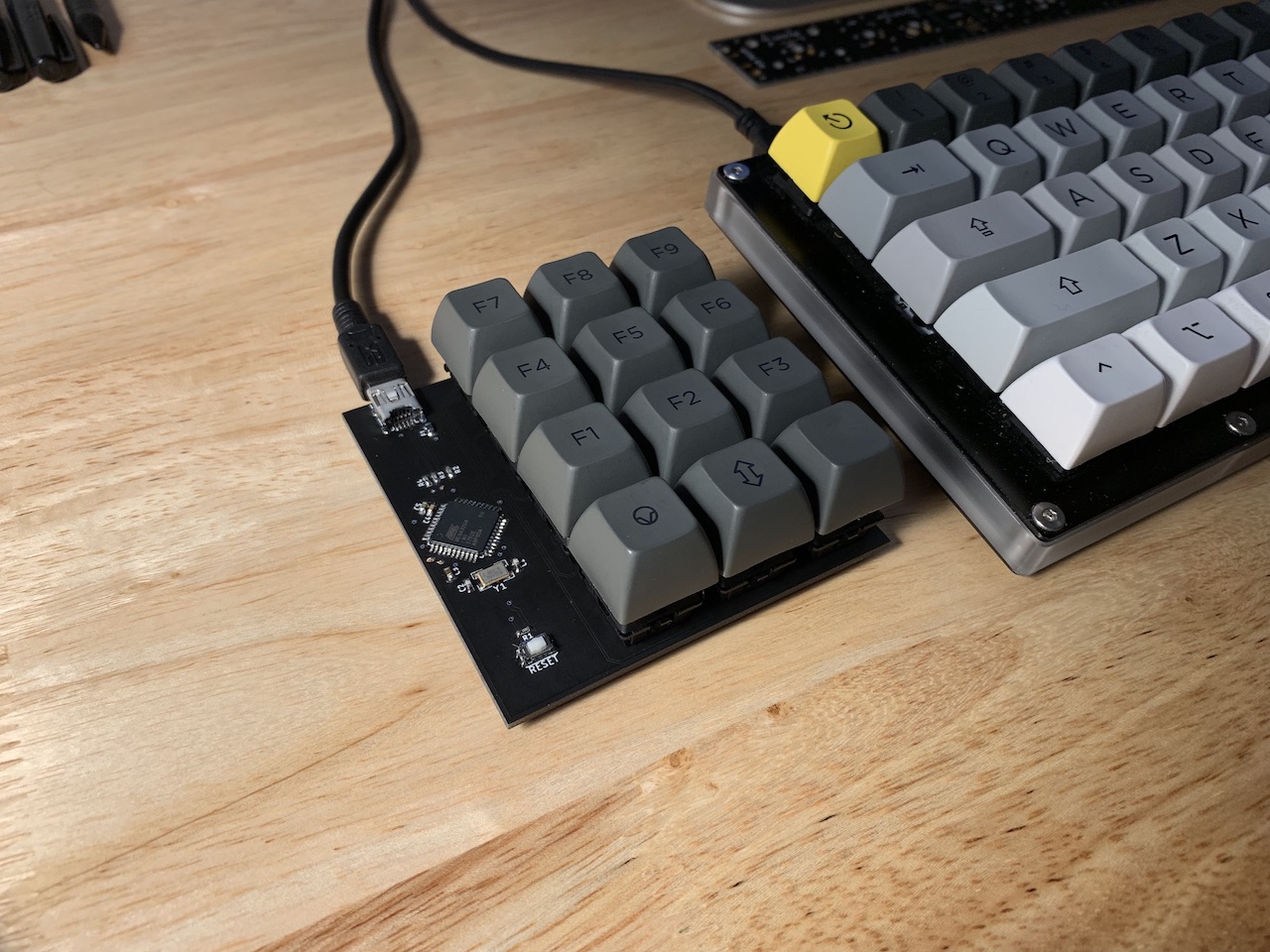
From this point on, it was just polish. I needed to spend a bit of time playing with QMK to get the key layout arranged like I wanted. I landed on a standard numberpad layout for the first layer with some modifier keys to jump up to the +-/* keys.
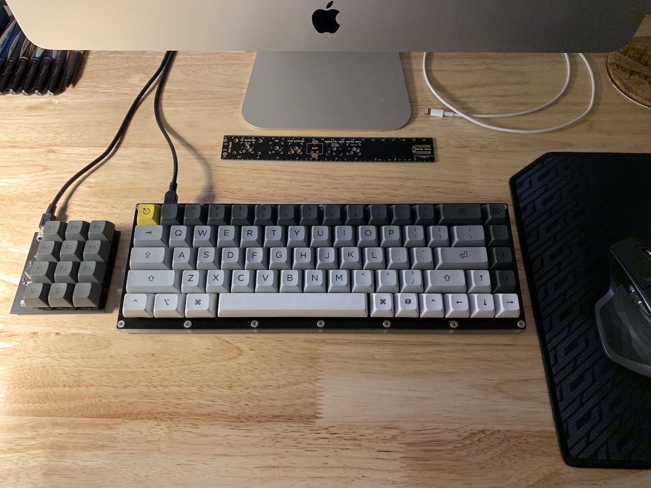
The board matches my full keyboard and is exactly what I designed it to be. This project was very different from my normal work, and was really rewarding. There’s something just plain fun about ending up with a physical device.
Any future boards should be significantly easier to design. I’ve learned quite a bit about circuit design, and about what makes a good keyboard. All in all, I wouldn’t recommend my macropad to anyone. It looks like I want, but it turns out that a single PCB really isn’t enough weight to keep something in place on my desk. The board slides all over the place whenever you press any of the keys. It’s a terrible tool to actually use.
If you’d like to learn more, the Eagle files, bill of materials, and QMK config is all available here.